- 您现在的位置:买卖IC网 > Sheet目录475 > MC13917-900EVK (Freescale Semiconductor)IC MC13917_900_EVK
Scattering and Noise Parameters
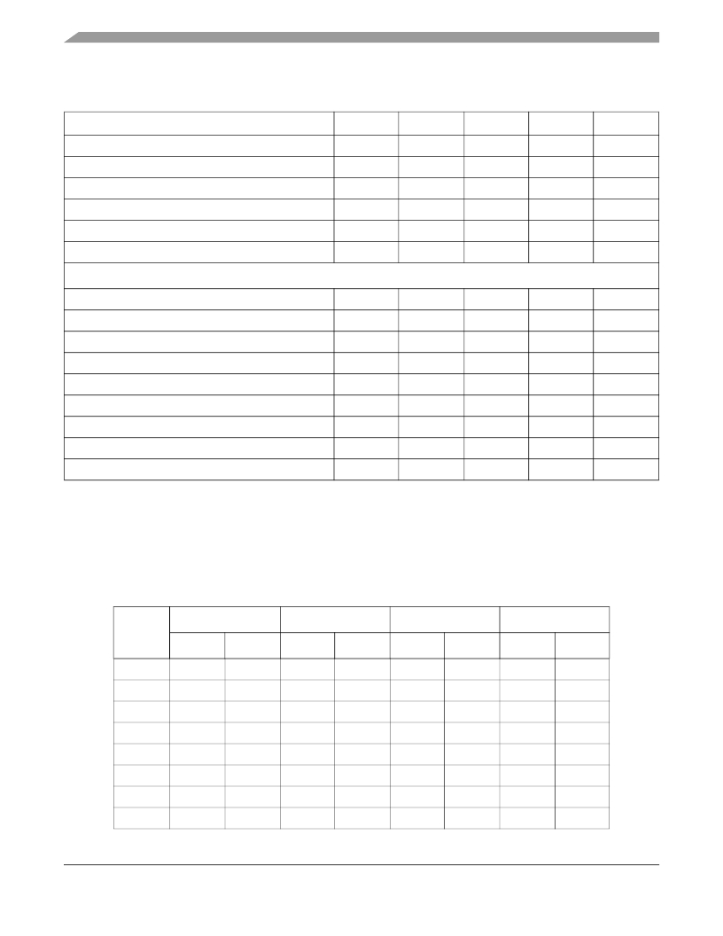
Table 4. Electrical Characteristics Measured in Frequency-Specific Tuned Circuits (continued)
(Vcc = 2.7V, T A = 25°C unless otherwise noted)
Characteristic
Output 3rd Order Intercept Point
Power Output at 1 dB Gain Compression
Input Return Loss
Small Signal Gain
Reverse Isolation
Output Return Loss
Symbol
OIP3
P1 dBoutput
S11
S21
S12
S22
Min
11
2
—
23
—
—
Typ
12.4
3.5
-10
24
-40
-23
Max
—
—
-9
—
-39
-16
Unit
dBm
dBm
dB
dB
dB
dB
1900 MHz (see Figure 19 )
Supply Current
RF Gain
Noise Figure
Output 3rd Order Intercept Point
Power Output at 1 dB Gain Compression
Input Return Loss
Small Signal Gain
Reverse Isolation
Output Return Loss
Icc
G
NF
OIP3
P1 dBoutput
S11
S21
S12
S22
—
13.5
—
7
-2.5
—
13.8
—
—
4.7
14.9
1.8
8.5
-1.1
-13
14.8
-42.5
-11.8
5.6
—
2.15
—
—
-10
—
-41.5
-10
mA
dB
dB
dBm
dBm
dB
dB
dB
dB
3
Scattering and Noise Parameters
Table 5 through Table 8 lists the S parameters for the packaged part in a 50 Ω system at four supply voltage
levels.
Table 5. Scattering Parameters
(Vcc = 2.7V, 25 ° C, 50 Ω system)
S11
S21
S12
S22
f (MHz)
Mag
Ang
Mag
Ang
Mag
Ang
Mag
Ang
100
150
200
250
300
350
400
450
0.864
0.859
0.843
0.831
0.812
0.794
0.775
0.754
-8.1
-12.4
-16.2
-20.6
-24.5
-28.3
-32.1
-35.7
12.178
12.428
12.112
12.128
11.95
11.741
11.556
11.353
169.9
165.1
160.5
156.1
151.8
147.9
143.8
140
0.001
0.001
0.001
0.002
0.002
0.002
0.002
0.003
24.4
36.2
39.4
52.1
52.6
59.2
64.2
66
0.953
0.952
0.951
0.952
0.951
0.95
0.947
0.947
-1.1
-1.5
-2.2
-2.8
-3.3
-4
-4.6
-5.4
MBC13917 Advance Information, Rev. 1.0
6
Freescale Semiconductor
发布紧急采购,3分钟左右您将得到回复。
相关PDF资料
MC1496P1
IC MODULATOR/DEMODULATOR 14-DIP
MC33493MOD868EV
BOARD EVAL MC33493 TANGO
MC33591MOD315EV
BOARD EVAL MC33493 TANGO3 RF
MC33593MOD868EV
BOARD EVAL MC33593 ROMEO2 RF
MC33690DWER2
IC STAND ALONE TAG READER 20SOIC
MC44CC375AVEFEVK
CCEVK NEJA EVAL KIT
MCH3374-TL-E
MOSFET P-CH 12V 3A MCPH3
MCH3375-TL-H
MOSFET P-CH 1.6A 30V MCPH3
相关代理商/技术参数
MC1391P
制造商:Motorola Inc 功能描述: 制造商: 功能描述: 制造商:undefined 功能描述:
MC13E-10-6PN
制造商:ITT Interconnect Solutions 功能描述:MC13E-10-6PN - Bulk
MC13E-10-6PW
制造商:ITT Interconnect Solutions 功能描述:MC13E-10-6PW - Bulk
MC13E-10-6SN
制造商:ITT Interconnect Solutions 功能描述:MC13E-10-6SN - Bulk
MC13E-10-6SN-A105
制造商:ITT Interconnect Solutions 功能描述:MC13E-10-6SN-A105 - Bulk
MC13E-13-12PN
制造商:ITT Interconnect Solutions 功能描述:MC13E-13-12PN - Bulk
MC13E-13-12SN
制造商:ITT Interconnect Solutions 功能描述:MC13E-13-12SN - Bulk
MC13E-8-3PN
制造商:ITT Interconnect Solutions 功能描述:MC13E-8-3PN - Bulk
